- 您现在的位置:买卖IC网 > Sheet目录342 > MCB11C14 (Keil)BOARD EVAL FOR NXP LPC11C14
�� �
�
�NXP� Semiconductors�
�LPC11C12/C14�
�[6]�
�[7]�
�[8]�
�[9]�
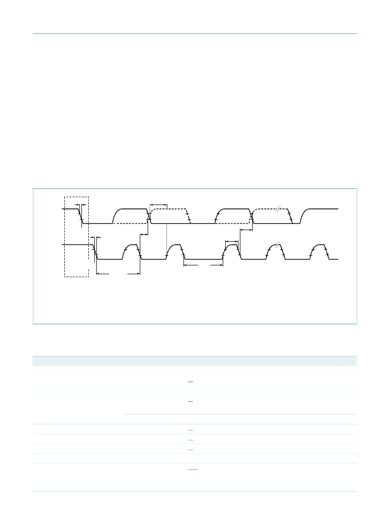
�The� maximum� t� f� for� the� SDA� and� SCL� bus� lines� is� specified� at� 300� ns.� The� maximum� fall� time� for� the� SDA�
�output� stage� t� f� is� specified� at� 250� ns.� This� allows� series� protection� resistors� to� be� connected� in� between� the�
�SDA� and� the� SCL� pins� and� the� SDA/SCL� bus� lines� without� exceeding� the� maximum� specified� t� f� .�
�In� Fast-mode� Plus,� fall� time� is� specified� the� same� for� both� output� stage� and� bus� timing.� If� series� resistors�
�are� used,� designers� should� allow� for� this� when� considering� bus� timing.�
�The� maximum� t� HD;DAT� could� be� 3.45� μ� s� and� 0.9� μ� s� for� Standard-mode� and� Fast-mode� but� must� be� less� than�
�the� maximum� of� t� VD;DAT� or� t� VD;ACK� by� a� transition� time� (see� UM10204� ).� This� maximum� must� only� be� met� if�
�the� device� does� not� stretch� the� LOW� period� (t� LOW� )� of� the� SCL� signal.� If� the� clock� stretches� the� SCL,� the�
�data� must� be� valid� by� the� set-up� time� before� it� releases� the� clock.�
�t� SU;DAT� is� the� data� set-up� time� that� is� measured� with� respect� to� the� rising� edge� of� SCL;� applies� to� data� in�
�transmission� and� the� acknowledge.�
�[10]� A� Fast-mode� I� 2� C-bus� device� can� be� used� in� a� Standard-mode� I� 2� C-bus� system� but� the� requirement� t� SU;DAT� =�
�250� ns� must� then� be� met.� This� will� automatically� be� the� case� if� the� device� does� not� stretch� the� LOW� period�
�of� the� SCL� signal.� If� such� a� device� does� stretch� the� LOW� period� of� the� SCL� signal,� it� must� output� the� next�
�data� bit� to� the� SDA� line� t� r(max)� +� t� SU;DAT� =� 1000� +� 250� =� 1250� ns� (according� to� the� Standard-mode� I� 2� C-bus�
�specification)� before� the� SCL� line� is� released.� Also� the� acknowledge� timing� must� meet� this� set-up� time.�
�t� f�
�t� SU;DAT�
�SDA�
�70� %�
�30� %�
�70� %�
�30� %�
�t� f�
�t� HD;DAT�
�t� H� IGH�
�t� VD;DAT�
�SCL�
�70� %�
�30� %�
�70� %�
�30� %�
�70� %�
�30� %�
�70� %�
�30� %�
�t� LOW�
�S�
�1� /� f� SCL�
�002aaf425�
�Fig� 19.� I� 2� C-bus� pins� clock� timing�
�10.6� SPI� interfaces�
�Table� 14.�
�Dynamic� characteristics� of� SPI� pins� in� SPI� mode�
�Symbol�
�T� cy(PCLK)�
�T� cy(clk)�
�Parameter�
�PCLK� cycle� time�
�clock� cycle� time�
�Conditions�
�[1]�
�Min�
�20�
�40�
�Typ�
�-�
�-�
�Max�
�-�
�-�
�Unit�
�ns�
�ns�
�SPI� master� (in� SPI� mode)�
�t� DS�
�data� set-up� time�
�in� SPI� mode�
�[2]�
�27�
�-�
�-�
�ns�
�2.0� V� ≤� V� DD� ≤� 3.6� V�
�1.8� V� ≤� V� DD� <� 2.0� V�
�36�
�-�
�-�
�ns�
�t� DH�
�data� hold� time�
�in� SPI� mode�
�[2]�
�0�
�-�
�-�
�ns�
�t� v(Q)�
�t� h(Q)�
�data� output� valid� time� in� SPI� mode�
�data� output� hold� time� in� SPI� mode�
�[2]�
�[2]�
�-�
�0�
�-�
�-�
�10�
�-�
�ns�
�ns�
�SPI� slave� (in� SPI� mode)�
�t� DS�
�data� set-up� time�
�in� SPI� mode�
�[3][4]�
�0�
�-�
�-�
�ns�
�LPC11C12_C14_0�
�Preliminary� data� sheet�
�All� information� provided� in� this� document� is� subject� to� legal� disclaimers.�
�Rev.� 00.05� —� 23� April� 2010�
�?� NXP� B.V.� 2010.� All� rights� reserved.�
�37� of� 49�
�发布紧急采购,3分钟左右您将得到回复。
相关PDF资料
MCB2470
BOARD EVAL NXP LPC247X SERIES
MCBSTM32EXL
BOARD EVALUATION FOR STM32F103ZE
MCBTMPM330
BOARD EVAL TOSHIBA TMPM330 SER
MCIMX25WPDKJ
KIT DEVELOPMENT WINCE IMX25
MCIMX53-START-R
KIT DEVELOPMENT I.MX53
MCM69C432TQ20
IC CAM 1MB 50MHZ 100LQFP
MCP1401T-E/OT
IC MOSFET DRVR INV 500MA SOT23-5
MCP1403T-E/MF
IC MOSFET DRIVER 4.5A DUAL 8DFN
相关代理商/技术参数
MCB11C14-ED
制造商:ARM Ltd 功能描述:KEIL NXP LPC11C14 EVAL BOARD
MCB11C14U
功能描述:开发板和工具包 - ARM EVAL BOARD FOR NXP LPC11C14 + ULINK2
RoHS:否 制造商:Arduino 产品:Development Boards 工具用于评估:ATSAM3X8EA-AU 核心:ARM Cortex M3 接口类型:DAC, ICSP, JTAG, UART, USB 工作电源电压:3.3 V
MCB11C14UME
功能描述:开发板和工具包 - ARM EVAL BOARD FOR NXP LPC11C14 + ULINK-ME
RoHS:否 制造商:Arduino 产品:Development Boards 工具用于评估:ATSAM3X8EA-AU 核心:ARM Cortex M3 接口类型:DAC, ICSP, JTAG, UART, USB 工作电源电压:3.3 V
MCB11C14UME-ED
制造商:ARM Ltd 功能描述:KEIL NXP LPC11C14 EVAL BOARD
MCB11U10
功能描述:开发板和工具包 - ARM EVAL BOARD FOR NXP LPC11U14
RoHS:否 制造商:Arduino 产品:Development Boards 工具用于评估:ATSAM3X8EA-AU 核心:ARM Cortex M3 接口类型:DAC, ICSP, JTAG, UART, USB 工作电源电压:3.3 V
MCB11U10U
功能描述:开发板和工具包 - ARM EVAL BOARD FOR NXP LPC11U14 + ULINK2
RoHS:否 制造商:Arduino 产品:Development Boards 工具用于评估:ATSAM3X8EA-AU 核心:ARM Cortex M3 接口类型:DAC, ICSP, JTAG, UART, USB 工作电源电压:3.3 V
MCB11U10U-ED
制造商:ARM Ltd 功能描述:KEIL NXP LPC11U10 EVAL BOARD
MCB11U10UME
功能描述:开发板和工具包 - ARM EVAL BOARD FOR NXP LPC11U14 + ULINK-ME
RoHS:否 制造商:Arduino 产品:Development Boards 工具用于评估:ATSAM3X8EA-AU 核心:ARM Cortex M3 接口类型:DAC, ICSP, JTAG, UART, USB 工作电源电压:3.3 V